
IC Layout
Top-Level Chip Layout
The layout and the micrograph of the die are shown in Fig.1.
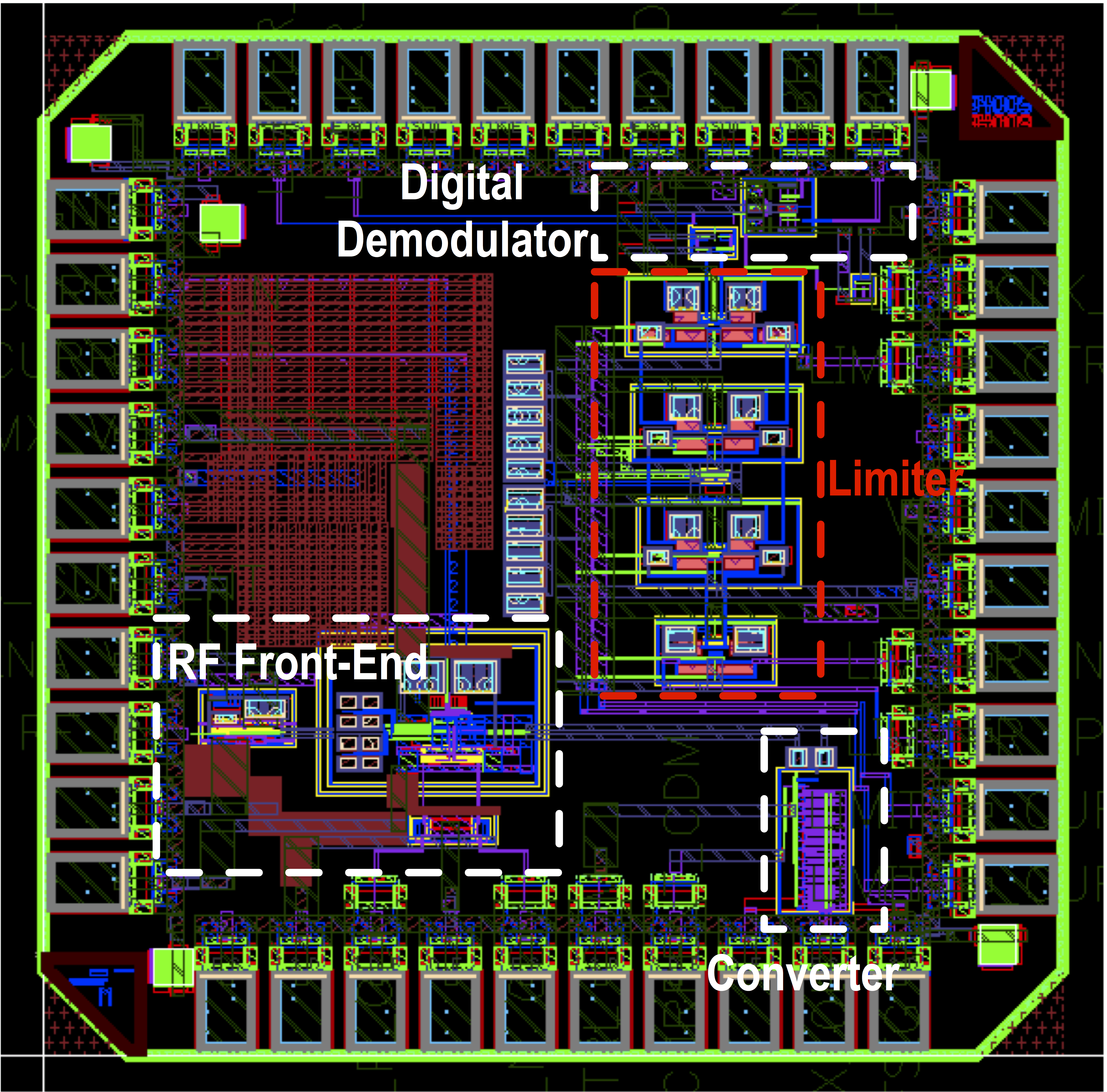
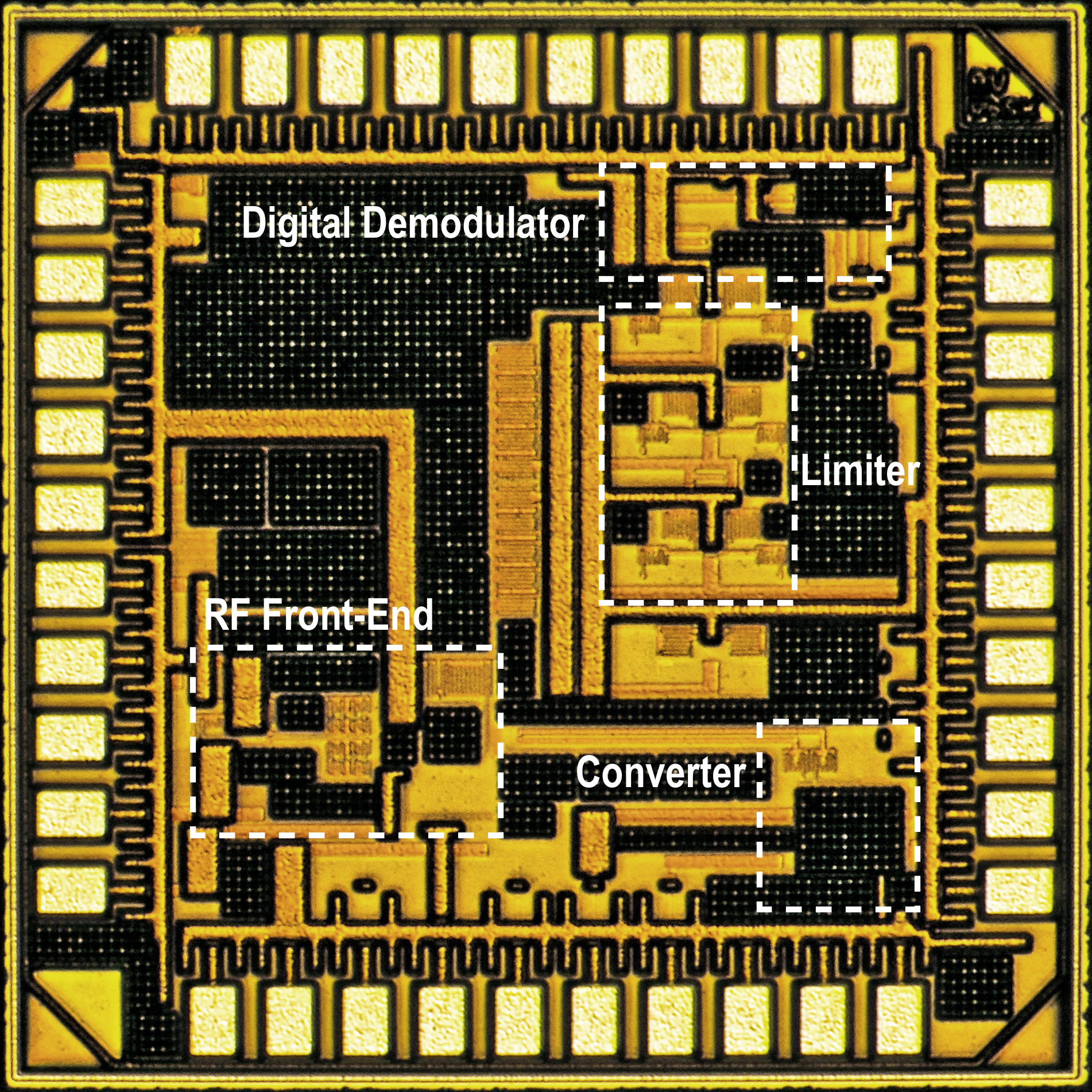
Fig.1 Layout and Micrograph of the Die
Low-Noise Amplifier (LNA)
Since the LNA is sensitive to parasitic capacitance, during layout, extra care was taken to mitigate parasitic effects caused by other blocks on the chip and by interconnections. Also, double-pattern guard rings have been employed to minimize substrate noise coupling. The RF transistors, provided in CMRF8RF library, were selected for their better modeling for parasitic capacitance. RF transistors have their gate fingers connected using M1 to reduce ohmic resistance instead of using poly-silicon.The layout of the LNA is shown in Fig.2.
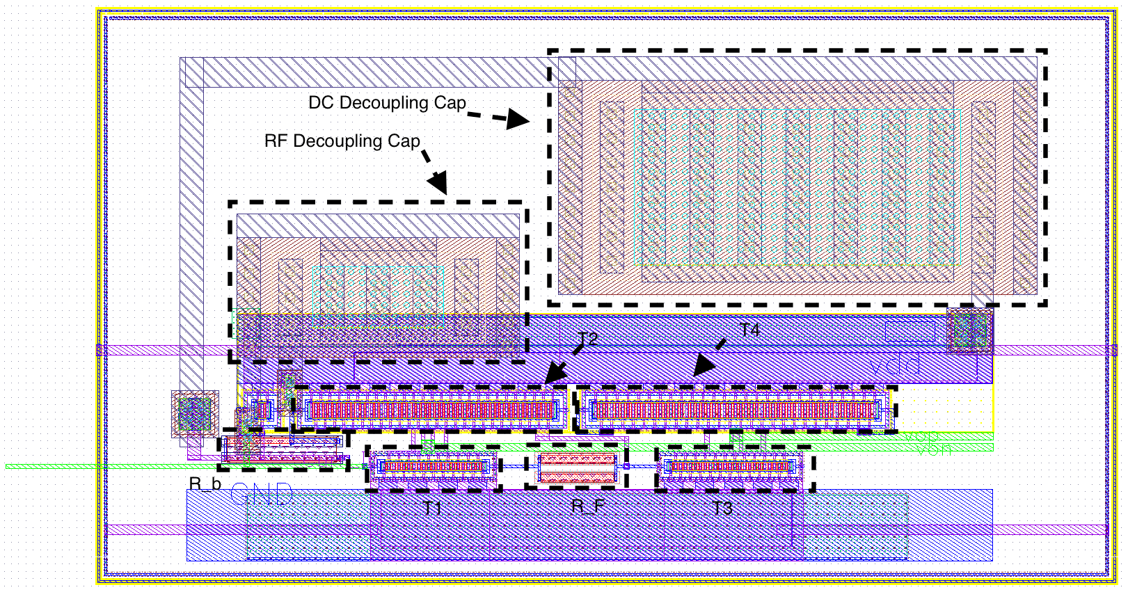
Fig.2 Layout of Low-Noise Amplifier
Double-Balanced Mixer
The layout of the mixer, shown in Fig.3, is designed to have RF signal wires and LO clock wires orthogonal to each other, so as to minimize the LO coupling to RF signals. Guard rings are employed to minimize the substrate coupling.
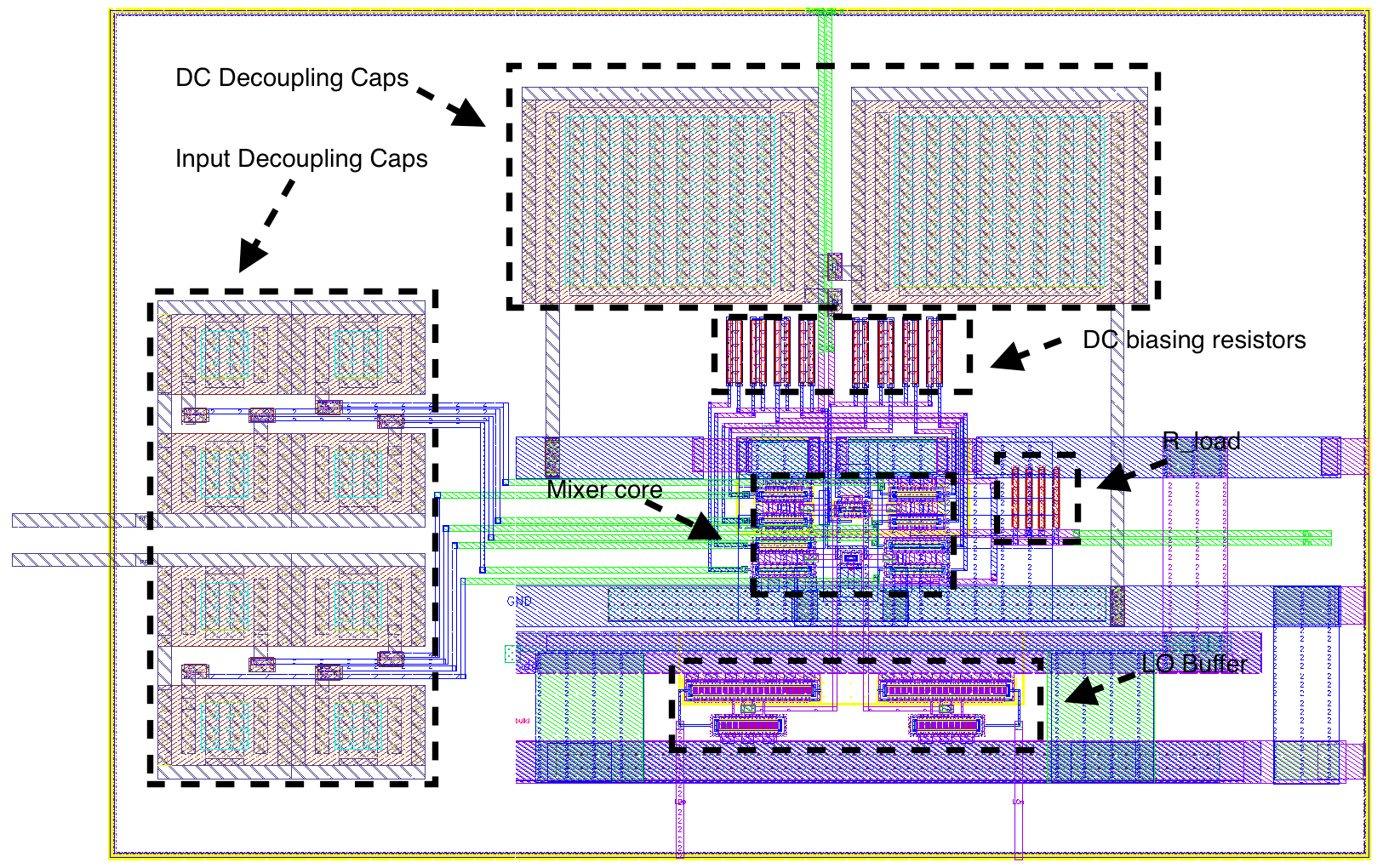
Fig.3 Layout of Double-Balanced Mixer
Differential-to-Single-Ended Converter
Since the output of the converter directly interfaces with the outside world, double-pattern guard rings are employed to protect NMOS transistors and single-pattern guard rings for PMOS transistors. The layout of the converter is shown in Fig.4.
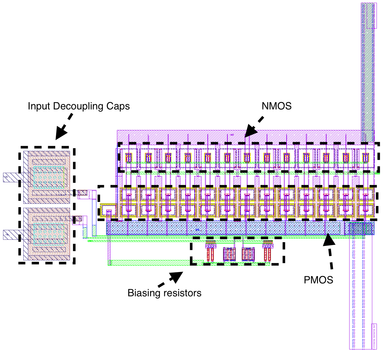
Fig.4 Layout of Differential-to-Single-Ended Converter
Limiting Amplifier
The limiting amplifier has very large voltage gain at one single frequency. There is a risk for parasitic oscillations. To mitigate this effect, the layout of the limiting amplifier is designed to be uni-directional, as shown in Fig.5. Guard rings are employed for each stage of the limiter to reduce substrate coupling.
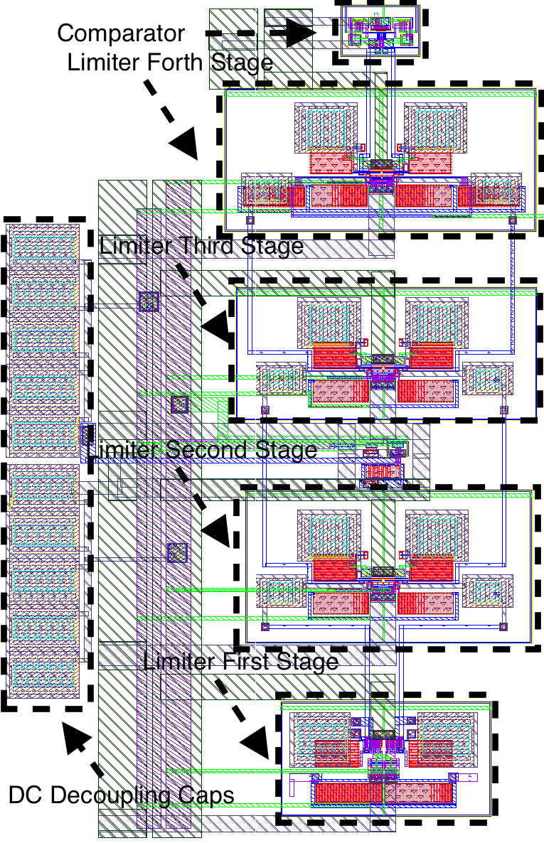
Fig.5 Layout of Limiting Amplifier
Digital Demodulator
The layout of the demodulator is also designed to be symmetric and uni-directional.
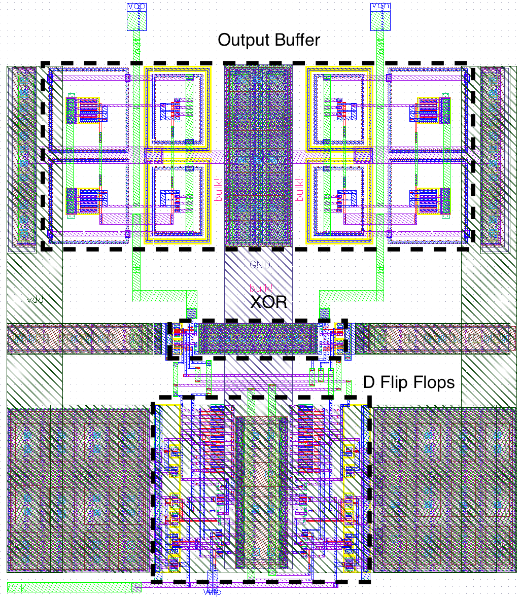
Fig.6 Layout of Digital Demodulator